Modern electronics depend on components that are smaller, faster, and more reliable than ever before. At the center of nearly every semiconductor package sits a critical structural and electrical element: the lead frame. Stamped lead frames have become the preferred solution for high-volume semiconductor production because they deliver the precision, repeatability, and electrical performance modern devices demand. As chip packaging continues to evolve, stamped lead frames remain a foundational technology that connects silicon to the outside world.
What Are Stamped Lead Frames?
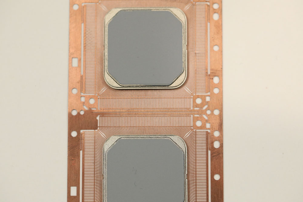
A lead frame is a thin metal structure that holds a semiconductor die in place and provides the electrical pathways between the chip and the circuit board. Stamped lead frames are produced through a high-speed metal stamping process that cuts and forms intricate patterns from a continuous strip of conductive material, typically copper alloys or specialty metals engineered for thermal and electrical performance.
Unlike etched lead frames, which are chemically processed, stamped lead frames are formed mechanically using progressive dies. This makes them ideal for high-volume production where consistency, speed, and cost efficiency matter most. The result is a component that meets exacting electrical specifications while remaining economical to produce at scale.
The Role of Stamped Lead Frames in Semiconductor Packaging
Semiconductor packages would not function without a reliable lead frame structure. Stamped lead frames serve three core purposes in modern chip packaging: they conduct electrical signals, dissipate heat away from the die, and provide the mechanical framework that holds everything together during assembly and use.
Electrical Conductivity and Signal Integrity
Stamped lead frames carry electrical signals between the semiconductor die and the printed circuit board. Because signal integrity is essential in high-frequency applications, the precision of the stamping process directly impacts performance. Tight tolerances and clean edges produced through precision metal stamping ensure that signal paths remain consistent across millions of identical parts.
Mechanical Support and Thermal Management
Beyond conductivity, stamped lead frames physically support the die during encapsulation and protect it from mechanical stress. They also act as a thermal pathway, helping move heat away from sensitive electronic components. Effective lead frame design balances electrical, mechanical, and thermal requirements in a single, integrated part.
How Precision Metal Stamping Produces High-Performance Lead Frames
The production of stamped lead frames starts with material selection and ends with inspection of finished parts on continuous reels. The process relies on high-speed progressive dies that perform multiple operations in a single pass. Each station in the die cuts, forms, or trims a specific feature, producing complete lead frames at speeds that can exceed 1,000 strokes per minute.
Precision metal stamping makes this scale possible while still holding the tight tolerances semiconductor packaging requires. Strip stock moves through the press in a continuous reel-to-reel format, which keeps parts aligned, protects them from handling damage, and allows downstream processes like plating to occur without removing parts from the carrier strip. This integrated approach is one of the main reasons stamped lead frames consistently outperform alternatives in high-volume environments.
Key Considerations in Lead Frame Design
Effective lead frame design is what separates a functional part from a high-performing one. Engineers must consider several factors before the first tool is built.
Material Selection
Copper alloys dominate lead frame production because they balance electrical conductivity, thermal performance, and formability. The exact alloy chosen depends on the end application, the required strength, and the plating system that will be applied later in the process.
Tolerance and Geometry
Semiconductor packages have shrunk dramatically over the past decade, and lead frame geometry has followed. Pitches are tighter, lead counts are higher, and feature sizes are smaller. Stamped lead frames produced by experienced manufacturers can hold the tolerances these designs require run after run.
Plating and Finish
Most lead frames require selective plating to support wire bonding, solderability, or corrosion resistance. Reel-to-reel plating, performed while parts remain on the carrier strip, delivers uniform coverage and protects critical surfaces before singulation.
Industries That Rely on Stamped Lead Frames
Stamped lead frames are found in nearly every sector that uses semiconductor devices. The industries most dependent on consistent, high-volume lead frame production include:
- Automotive electronics, including power management modules and sensor packages
- Consumer electronics, where compact, high-density packaging is standard
- Industrial automation and power systems requiring high-current capability
- Telecommunications and networking infrastructure
- Medical electronics that demand long-term reliability
- Aerospace and defense applications with strict performance requirements
Each of these industries depends on lead frame design that aligns with both the chip and the broader assembly process.
Why Choose a High-Speed Stamping Partner for Lead Frame Production
Producing stamped lead frames at scale is not just about owning a press. It requires integrated tool and die capability, deep material knowledge, and quality systems built around tight-tolerance work. A capable manufacturing partner handles every step in-house, from initial lead frame design support and tooling fabrication through high-speed production, plating, and final inspection.
This vertical integration reduces variation, shortens lead times, and keeps quality control under one roof. For engineers sourcing stamped lead frames, working with a partner that owns the full process means fewer handoffs, fewer opportunities for defects, and a faster path from prototype to full production. It also creates room for collaboration during the design phase, where small changes to lead frame design can have a significant impact on manufacturability and long-term part performance.
The Future of Stamped Lead Frames in Semiconductor Manufacturing
As semiconductor packaging continues to advance, demand for stamped lead frames will grow alongside it. Power electronics, electric vehicles, and next-generation communication systems are all driving the need for lead frames that can handle higher currents, finer pitches, and more demanding thermal conditions. Precision metal stamping is well positioned to meet these requirements because it scales efficiently and maintains tight process control across millions of parts.
Innovations in materials, tooling, and inline inspection are pushing the performance envelope further, making stamped lead frames a continued cornerstone of modern electronics manufacturing.
Powering the Next Generation of Electronics
Stamped lead frames are more than a structural component. They are the connection point between the silicon that powers modern devices and the circuit boards that bring those devices to life. With precision metal stamping, thoughtful lead frame design, and integrated manufacturing capabilities, stamped lead frames will continue to support the performance, reliability, and scale that semiconductor packaging demands.